Английский Наука и Образование
12.08.2026 Читать источник
Плазмоника повысит эффективность инфракрасных детекторов на основе HgCdTe
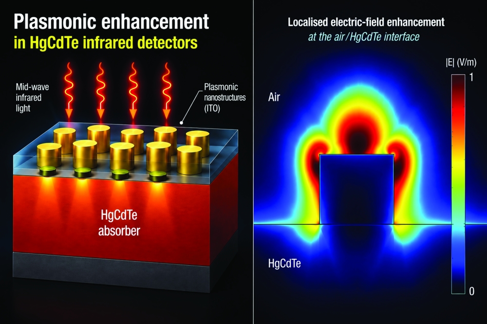
Исследователи из Университета штата Теннесси продемонстрировали, что плазмонные наноструктуры усиливают поглощение среднего инфракрасного излучения на 15–18% без изменения толщины полупроводника. Данная технология позволяет повысить чувствительность и разрешение детекторов за счет усиления локального электрического поля в активном слое.
Перевод ИИ
Текст статьи доступен на языке оригинала.
Нажмите кнопку «Перевести статью» выше, чтобы сгенерировать перевод с помощью ИИ.
Оригинальный контент
Enhancing HgCdTe detectors with plasmonics
With the addition of plasmonic nanostructures, HgCdTe
infrared detectors can benefit from stronger signals and provide several
advantages at the system level.
BY NAGENDRABABU VANAMALA FROM TENNESSEE STATE UNIVERSITY
While they are often unseen, infrared detectors are all around us, underpinning many applications. They are deployed for night vision, surveillance and environmental monitoring, and advanced defence systems.
For detection in the infrared, the established material of choice is HgCdTe. Merits of this ternary include its tuneable bandgap, and its high sensitivity across a wide spectral range.
While these advantages are valued, there’s a fundamental challenge with HgCdTe. When incident infrared radiation impinges on this detector’s active region, the resulting interaction may not be strong enough to generate a large population of charge carriers. This weakness stems from an optical absorption that is not that high, holds back signal strength, and ultimately constrains detector sensitivity and resolution.
Due to this limitation, strategies for improving detector performance must focus on enhancing the light-matter interaction within the absorber. An attractive way to realise this is to strengthen the local electric-field intensity, as this increases the efficiency for the conversion of incoming photons into electrical signals, without having to increase absorber thickness or adjust semiconductor composition.
HgCdTe foundations
By altering the composition of HgCdTe, detection can span the short-wave, mid-wave, and long-wave spectral regions. This flexibility makes this alloy indispensable for multispectral and broadband sensing systems operating across atmospheric transmission windows.
Traditionally, to ensure strong absorption, the designers of detectors employ relatively thick absorber layers. While this strategy enables effective capture of photons, thicker material may exacerbate recombination effects and impose constraints on performance, manufacturability and cost. All this matters – there’s demand for infrared systems with superior sensitivities and greater efficiencies, so enhancing absorption without increasing material thickness is a central challenge.
Approaches to tackling this need to enhance absorption include modifying the semiconducting material. But there’s also a more elegant solution, involving engineering of the optical environment at the detector surface.
That’s the methodology we’re pursuing at Tennessee State University. Our efforts demonstrate that it’s possible to significantly enhance midwave infrared absorption in HgCdTe by integrating plasmonic nanostructures at the detector interface. By adding carefully designed metallic or dielectric nanostructures, our design concentrates optical fields near the surface, strengthening the light-matter interaction and increasing absorption within the active region.
Field enhancement
When infrared radiation interacts with our nanostructures, this generates collective oscillations of free electrons, known as surface plasmons. These resonances introduce highly localised electromagnetic fields in the vicinity of the nanostructures. In turn, there’s an increase in the optical energy density inside the HgCdTe absorber, boosting photon absorption within thinner layers. According to numerical modelling by our team, optimised plasmonic structures enhance midwave infrared absorption by approximately 15-18 percent, with higher gains achievable for specific geometries. Crucially, this enhancement comes without increasing absorber thickness or modifying the semiconductor material.
We employ what’s referred to as an effective-medium approach to model the optical response of nanostructured HgCdTe systems. Although structures involve nanoscale features, so quantum effects influence carrier behaviour, one can treat the interaction with infrared radiation with classical electromagnetic theory.
The structures we have considered include periodic nanostructure arrays, consisting of materials such as indium tin oxide embedded in air – it’s a combination that forms an effective optical layer, with a refractive index depending on geometry, spacing, and scattering characteristics. The effective index, which is strongly dependent on feature size, periodicity, and geometry, governs the resulting electric-field distribution, quantum efficiency, and absorption behaviour.
To ensure plasmonic enhancement, nanostructured material must exhibit a negative real permittivity at the detector’s operating wavelength. In the mid-wave infrared, there are a number of transparent conducting oxides satisfying this condition, behaving as metallic media while maintaining a comparatively low optical loss. When this happens, localised surface plasmons are excited at the interface with HgCdTe, producing intense near-field confinement and a strong coupling of optical energy into the absorber. This allows transparent conducting oxides to serve as effective plasmonic materials in spectral domains where conventional noble metals are less suitable.
The negative permittivity, needed to ensure a plasmonic resonance, governs how electromagnetic waves are confined and guided at the nanostructure interface. A negative permittivity ensures that the material supports surface-bound modes – they remain tightly confined near the interface rather than propagating into free space. Thanks to this confinement, there’s a significant increase in the local density of optical states, allowing more-efficient coupling of incident radiation into the absorber region.
From a device perspective, this behaviour is ideal, as it enhances the probability that photons contribute to carrier generation, and it reduces the likelihood that they are reflected or transmitted. The upshot is more efficient optical-to-electrical conversion, even in thin absorbers. It’s an improvement that’s particularly important in HgCdTe systems, where absorption, noise figures, and detector sensitivity are strongly linked to absorber thickness.
During our development of HgCdTe detectors that are enhanced with plasmonics, we uncovered small deviations between our measured and simulated values for absorption near the band edge, arising primarily from temperature sensitivity and detector operating conditions. Note that HgCdTe devices are typically optimised for low-temperature operation, and measurements performed under ambient conditions introduce fluctuations in detector response. This is particularly significant near the absorption edge, where small temperature variations may lead to noticeable differences in measured absorbance.
Why geometry matters
Details associated with geometry play a crucial role in determining how effectively plasmonic structures enhance absorption. We have shown that while the choice of material sets the fundamental electromagnetic response, the spatial distribution and intensity of the near field are governed by the shape and periodic arrangement of the nanostructures.
Аналитика ИИ и парсинга
Технические детали обнаружения, сопоставления и связывания статьи
Поисковый запрос
«плазмоника инфракрасные детекторы HgCdTe эффективность»
Запрос, сгенерированный ИИ для поиска статьи в веб-источниках
Связанные результаты поиска
Результаты поиска отсутствуют в БД
Парсер не сохранил результаты веб-поиска для этой статьи.